lipflip – A research team from Fudan University has achieved a major breakthrough in semiconductor technology. They have successfully integrated atomically thin 2D memory modules with a conventional silicon chip. This innovation marks the creation of the world’s first fully functional 2D-CMOS chip. Which could pave the way for smaller, faster, and more powerful electronic devices.
Read More : Tesla Model 3 Premium Gains Front Camera and $595 Stalk Upgrade
Led by Chunsen Liu at Fudan University in Shanghai, the team has successfully demonstrated how 2D materials can be combined with traditional silicon chips. As a result, their work, published in the journal Nature, bridges the gap between the theoretical potential of 2D materials and their practical application in real-world devices. Consequently, this breakthrough opens up new possibilities for integrating cutting-edge materials into mainstream technology.
For decades, engineers have been focused on shrinking the circuits in silicon chips. However, this approach is now reaching its physical limits. The development of 2D materials, which are just a single layer of atoms thick, presents a promising solution. However, integrating these fragile and unstable materials with conventional processors has posed significant challenges.
Overcoming Challenges: The Atom2Chip Technology
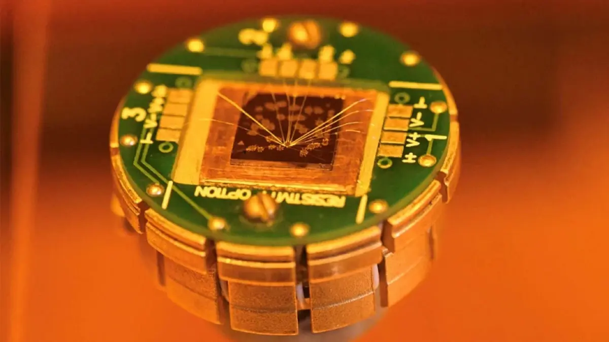
To address these challenges, the Fudan University team introduced a new technology called Atom2Chip. This innovation includes several key advancements to ensure the successful integration of 2D materials with silicon chips. The Atom2Chip technology features a full-stack on-chip process that allows a monolayer of molybdenum disulfide, a 2D material, to adhere to the rough surface of a CMOS chip. Special packaging techniques protect the fragile atomic layer, ensuring its stability.
The researchers also developed a cross-platform system that enables seamless communication between the 2D circuits and the mature CMOS platform. This breakthrough is not just a prototype; the team has created a fully functional 1-Kb 2D NOR flash memory chip that can perform complex. Instruction-driven operations.
In testing, the hybrid chip achieved an impressive clock speed of 5 MHz and demonstrated quick programming and erasing speeds of just 20 nanoseconds. Moreover, it consumed minimal energy, highlighting its potential for energy-efficient, high-performance memory devices.
Read More : Philips Hue Launches New Features in Latest Bridge Update
This achievement marks a significant step forward in developing next-generation memory technology. The 2D flash chip increases density and improves energy efficiency compared to current alternatives. While the current demonstration focuses on data storage, researchers believe they can eventually apply this approach to processors. This shift could lead to faster, thinner, and more power-efficient devices. Such advancements will likely revolutionize a wide range of technologies, from smartphones to artificial intelligence systems, by enabling faster processing speeds, reducing power consumption, and creating more compact form factors. This research opens exciting possibilities for the next era of computing devices.